
Description
Product Overview
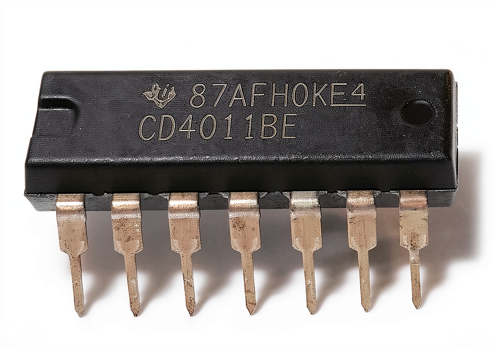
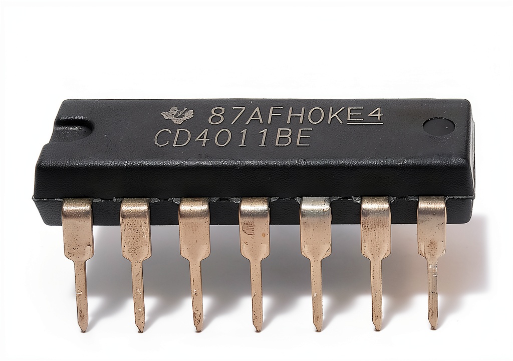
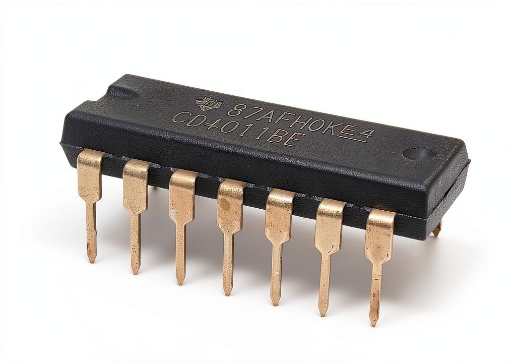
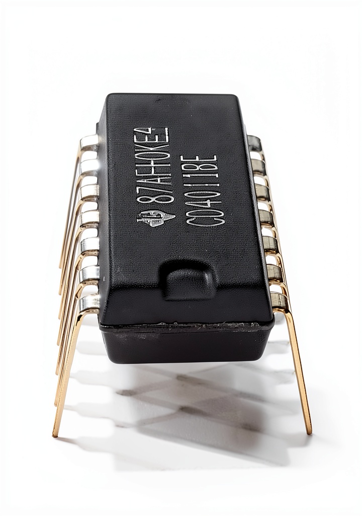
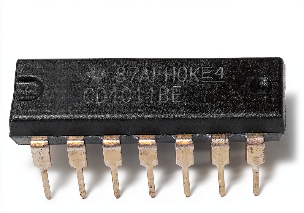
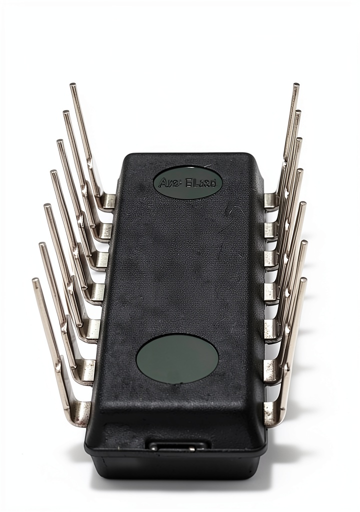
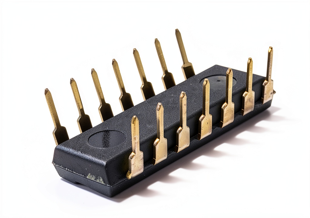
The CD4011BE from Texas Instruments is a high‑performance CMOS quad 2‑input NAND gate integrated circuit designed for a wide range of digital logic applications. Housed in a standard 14‑lead DIP package, the device offers four independent NAND gates that can be used individually or combined to create more complex logic functions. Each gate features buffered inputs and outputs, providing robust noise immunity and consistent switching behavior across the full operating voltage range of 5 V to 15 V. The IC’s propagation delay of 60 ns (typical at 10 V, 50 pF load) ensures rapid response times, while the low quiescent current of less than 1 µA at 18 V helps to minimize power consumption in battery‑powered or energy‑sensitive designs. The part complies with JEDEC Tentative Standard No. 13B, guaranteeing that it meets industry‑wide specifications for reliability, temperature stability, and electrical performance.
Designed with the needs of both hobbyists and professional engineers in mind, the CD4011BE provides a versatile platform for prototyping, educational projects, and production‑grade circuitry. The DIP‑14 footprint is compatible with standard breadboards, socket strips, and automated assembly equipment, allowing for quick insertion and removal during iterative design cycles. The device’s input leakage current is limited to 1 µA at 18 V, and as low as 100 nA at 18 V and 25 °C, which reduces the risk of unintended loading on preceding stages. Noise margins are generous, offering 1 V at a 5 V supply, 2 V at 10 V, and 2.5 V at 15 V, ensuring reliable operation even in noisy environments. The symmetrical output characteristics simplify interfacing with other logic families, making the CD4011BE a convenient bridge between older TTL logic and modern CMOS designs.
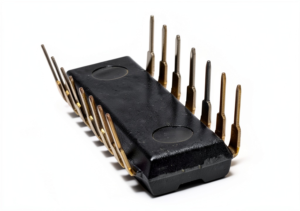
The manufacturing quality of the CD4011BE is backed by Texas Instruments’ extensive testing and quality assurance processes. Each IC undergoes 100 % functional verification at the rated supply voltage of 20 V, confirming that the quiescent current and switching parameters meet the specified limits. The package is constructed from a lead‑frame and epoxy resin that provide mechanical strength and protection against moisture and contaminants. Thermal performance is optimized for operation from –55 °C to +125 °C, allowing the component to function reliably in harsh industrial, automotive, and aerospace environments. The device’s robust construction also contributes to a long mean time between failures (MTBF), which is a critical factor for systems that require high uptime and minimal maintenance.
The CD4011BE’s electrical specifications are engineered for consistency across a broad spectrum of operating conditions. With a maximum supply voltage of 20 V, the device can tolerate transient spikes that commonly occur in industrial power environments. The output high voltage (VOH) remains within 0.9 × VDD, while the output low voltage (VOL) stays below 0.1 × VDD, guaranteeing clear logic levels for downstream circuitry. The input capacitance is limited to 5 pF, reducing the loading effect on high‑frequency signals. Additionally, the device’s propagation delay varies minimally with temperature, changing by less than 10 ns across the –55 °C to +125 °C range, which simplifies timing analysis in temperature‑sensitive designs.
The 14‑pin DIP package follows the standard pinout for quad NAND gates, making it instantly recognizable to engineers familiar with the 4011 family. Pins 1, 2, and 3 constitute the first NAND gate, with pin 1 and pin 2 as inputs and pin 3 as the output. This pattern repeats for the remaining three gates, while pins 7 and 14 serve as the VSS (ground) connections, and pins 8 and 13 provide the VDD supply. The symmetrical layout facilitates straightforward wiring on breadboards and printed circuit boards, reducing the chance of misconnection. For high‑density designs, the pins can be routed to surface‑mount equivalents using standard adapter boards, preserving the same electrical performance while saving board space.
Each CD4011BE undergoes rigorous reliability testing, including high‑temperature operating life (HTOL) and temperature cycling, to verify long‑term stability. The devices are screened for parametric compliance at both the nominal and extreme supply voltages, ensuring that the propagation delay, output drive strength, and leakage currents remain within specification. The ICs also pass electrostatic discharge (ESD) tests up to 2 kV, protecting them from damage during handling and assembly. These comprehensive test procedures contribute to a low field failure rate, which is essential for mission‑critical applications where downtime is costly.
Usage
The CD4011BE excels in a variety of usage scenarios, ranging from simple switch debouncing circuits to more sophisticated state machines and arithmetic logic units. Its four NAND gates can be wired to implement NAND‑based universal logic, enabling designers to build any Boolean function without needing additional gate types. Common applications include pulse‑width modulation (PWM) generators, frequency dividers, edge‑detecting circuits, and programmable logic arrays. Because the IC operates efficiently at both 5 V and 15 V, it can be integrated into low‑power microcontroller projects as well as higher‑voltage industrial control panels. The breadboard‑friendly pin layout makes it a favorite among educators teaching digital electronics, while the reliable performance satisfies the stringent requirements of commercial product development.
In addition to traditional digital logic, the CD4011BE can be employed in mixed‑signal designs where analog and digital sections coexist. For instance, the NAND gates can be used to shape analog waveforms, create timing windows, or generate clean digital control signals from noisy sensor inputs. The device’s low input current and high noise margin make it suitable for interfacing with high‑impedance sensors, such as photodiodes or resistive temperature detectors, without loading the source. Its ability to operate over a wide temperature range also enables deployment in outdoor instrumentation, automotive control units, and industrial automation equipment where environmental conditions fluctuate dramatically.
When integrating the CD4011BE into a larger system, careful attention to power distribution and decoupling is essential. Placing a 0.1 µF ceramic capacitor close to the VDD and VSS pins of each IC helps suppress supply noise and improves transient response. For high‑speed applications, keep the trace lengths of the input and output signals as short as possible and use controlled‑impedance routing to maintain signal integrity. If multiple NAND gates are required to operate synchronously, consider using a common clock source and matching the load capacitance on each output to achieve uniform propagation delays across the gates.
The breadboard‑friendly nature of the CD4011BE makes it an excellent choice for rapid prototyping and educational labs. Designers can quickly assemble test circuits to evaluate timing characteristics, logical behavior, and power consumption without the need for custom PCBs. Oscilloscope measurements of the propagation delay and output swing can be performed directly on the breadboard, allowing for immediate verification against the datasheet specifications. Once the design is validated, the same schematic can be transferred to a printed circuit board with minimal modifications, streamlining the transition from prototype to production.
Modern microcontrollers often operate at 3.3 V or 5 V logic levels, and the CD4011BE can be interfaced with these devices by ensuring that the supply voltage matches the logic level of the microcontroller. When used at a 5 V supply, the NAND gate outputs are fully compatible with 5 V tolerant I/O pins, while at 3.3 V operation, the device still provides sufficient noise margin for reliable communication. Level‑shifting circuits or pull‑up resistors can be added if the downstream logic requires higher voltage thresholds, making the CD4011BE a flexible bridge between legacy CMOS logic and contemporary digital platforms.
Why Choose Us
Choosing the CD4011BE from Texas Instruments means selecting a component that combines proven reliability with flexible functionality. TI’s global support network provides comprehensive documentation, reference designs, and application notes that help engineers accelerate development and reduce time‑to‑market. The part’s availability in a pack of eight ensures that designers have sufficient inventory for both prototype builds and small‑volume production runs, while the competitive pricing of $13.49 per pack offers cost‑effective scaling. Moreover, TI’s commitment to sustainability and responsible manufacturing aligns with modern corporate environmental goals, giving customers confidence that their supply chain adheres to ethical standards.
The CD4011BE’s design emphasizes ease of use without sacrificing performance. Buffered inputs reduce the need for external pull‑up or pull‑down resistors, simplifying circuit layouts and saving board space. The symmetrical output drive capability allows the gates to source and sink comparable currents, facilitating direct interfacing with both TTL and CMOS logic families. Additionally, the device’s low propagation delay supports high‑speed switching applications, while the generous noise margins protect against spurious transitions caused by electromagnetic interference (EMI). Together, these attributes provide a balanced solution that meets the demands of both novice makers and seasoned professionals.
TI’s global manufacturing footprint and diversified supply chain reduce the risk of component shortages and lead‑time delays. The CD4011BE is stocked in multiple regional distribution centers, ensuring that customers receive consistent product availability regardless of geographic location. This reliability is especially valuable for manufacturers with just‑in‑time (JIT) production schedules, as it minimizes inventory holding costs while maintaining uninterrupted assembly lines. In addition, TI provides real‑time visibility into inventory levels through its online portal, allowing purchasers to plan orders proactively.
Beyond the hardware, Texas Instruments offers an extensive library of application notes, reference designs, and simulation models that accelerate development cycles. Engineers can access SPICE models for the CD4011BE to perform circuit simulations before hardware prototyping, reducing trial‑and‑error iterations. TI’s technical support team is available to answer design‑specific questions, troubleshoot performance issues, and suggest optimal layout practices. This level of assistance helps customers achieve design success faster and with greater confidence.
TI is committed to sustainable manufacturing practices, including waste reduction, energy efficiency, and responsible sourcing of raw materials. The CD4011BE is produced in facilities that adhere to ISO 14001 environmental management standards, ensuring that the component’s lifecycle impact is minimized. Customers seeking to meet their own corporate social responsibility (CSR) goals can rely on TI’s transparent reporting and compliance certifications, which simplify the process of documenting environmental stewardship throughout the supply chain.
Purchasers of the CD4011BE benefit from a comprehensive warranty and a responsive after‑sales service network. Should any issues arise, TI’s customer service can provide replacement units, technical guidance, and, if necessary, expedited shipping to minimize downtime. The company also offers a robust return‑to‑vendor (RTV) program for defective parts, ensuring that quality concerns are addressed promptly and efficiently.
Key Features
- Four independent NAND gates in a single DIP‑14 package simplify circuit design and reduce component count.
- Typical 60 ns propagation delay delivers fast switching for high‑speed digital applications.
- Low input leakage (≤1 µA) minimizes power draw, ideal for battery‑operated and low‑power systems.
- Broad operating voltage (5 V‑15 V) and wide temperature range (‑55 °C to +125 °C) ensure reliable performance in diverse environments.
- TI’s extensive support and 100 % tested quality provide confidence, backed by responsive customer service and after‑sales assistance.
FAQ
What is the maximum fan‑out for the CD4011BE?
The device can drive up to 10 standard CMOS inputs at 5 V, and up to 5 TTL inputs, while maintaining reliable logic levels.
Can the CD4011BE be used in 3.3 V systems?
Yes, the IC operates correctly down to 5 V; for 3.3 V operation, ensure that the input voltage does not exceed the supply voltage and consider using level‑shifting circuitry if needed.
Is the CD4011BE suitable for automotive applications?
The part’s automotive‑grade temperature range (‑55 °C to +125 °C) and robust JEDEC compliance make it appropriate for many automotive control modules, provided that the circuit meets the required isolation and protection standards.
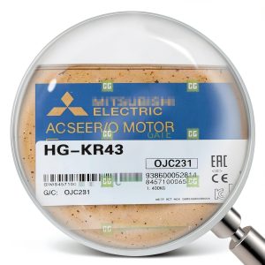 HG-KR43 ONE New HG-KR43 for Delivery
Reviews
There are no reviews yet.